Research project
ALPIDE Bending Tests Related to ALICE ITS3 WP4
An 18 mm bending fixture and test workflow
Institution
HIPEx Group, Pusan National University
Collaboration
ALICE ITS3 WP4-related activities
Timeline
Mar 2023 - Jan 2024
Project Overview
My scope as an undergraduate researcher
ALICE is an experiment at the LHC that studies heavy-ion collisions, and it relies on an Inner Tracking System (ITS) to reconstruct particle trajectories near the interaction point with high precision. Tracking performance depends strongly on how close the innermost sensor layer sits to the interaction point and how little material the particles have to pass through. ITS3 is an upgrade that aims to rework this innermost region by bending a single, wafer-scale monolithic active pixel sensor (MAPS) into a half-cylinder that wraps around the beam pipe, instead of mechanically assembling many modules. Doing so reduces the supports and coolant and lowers the that particles cross close to the interaction point. For this design to work, however, one has to confirm whether a silicon sensor still operates correctly and keeps its characteristics once it is actually bent — and the bending fixture, readout setup, and standard scans documented on this page are the local unit within that verification effort.
More specifically, ITS3 replaces the three innermost layers of ITS2 with thin, wafer-scale silicon sensors and uses lightweight supports together with air cooling. The three layers have nominal bending radii of about 18, 24, and 30 mm, and the fixture covered on this page targets the innermost of them, roughly 18 mm.
As an undergraduate researcher in the HIPEx group at Pusan National University, I worked on the fixture and measurement procedure for bending and testing a thinned -and-FPC assembly. These included dummy-chip mounting trials, design of the PNU Guide & Frame, 3D profile measurement, readout setup, and execution of standard scans in flat, bent, and reverse-bent configurations.
Scope of this page
This page documents only the design, setup, and measurement procedure of the work I carried out. It does not present measured values, differences between configurations, trends, the presence or absence of effects, physical interpretations, or conclusions, since these have not undergone peer review.

The test ALPIDE used a Carrier Board wire-bonded to an that the koALICE team designed and Memspack in Korea fabricated. It connects to the through an iBoard and Adapter Board.
I received this sample, connected this readout chain, and prepared the test setup so the same procedure could be used to scan it in the bent state as well.
PNU Guide & Frame
An 18 mm bending fixture for handling the FPC
The early work used an (about 30 × 15 × 0.05 mm) together with Kapton tape to examine different mounting positions and contact areas. With a deliberately small taping area, the dummy chip stayed fixed on an 18 mm cylinder for weeks, showing how little adhesive the approach needed. I then designed and printed a two-part Guide and Frame so that the FPC could be positioned on the support while minimizing direct handling of the sensor surface and wire bonds.
The Frame used in this work had a nominal bending radius of 18 mm, and this page limits its fixture and test description to that condition.

The Frame was designed to provide a surface with a nominal radius of 18 mm, while the Guide was designed to position the FPC as it was inserted toward the Frame.
After fabrication, I used a Keyence VR-6200 3D optical measurement system to inspect the surface profile of the mounted dummy chip and compare it with the intended geometry. This page does not present numerical outputs or a tolerance assessment from that measurement.
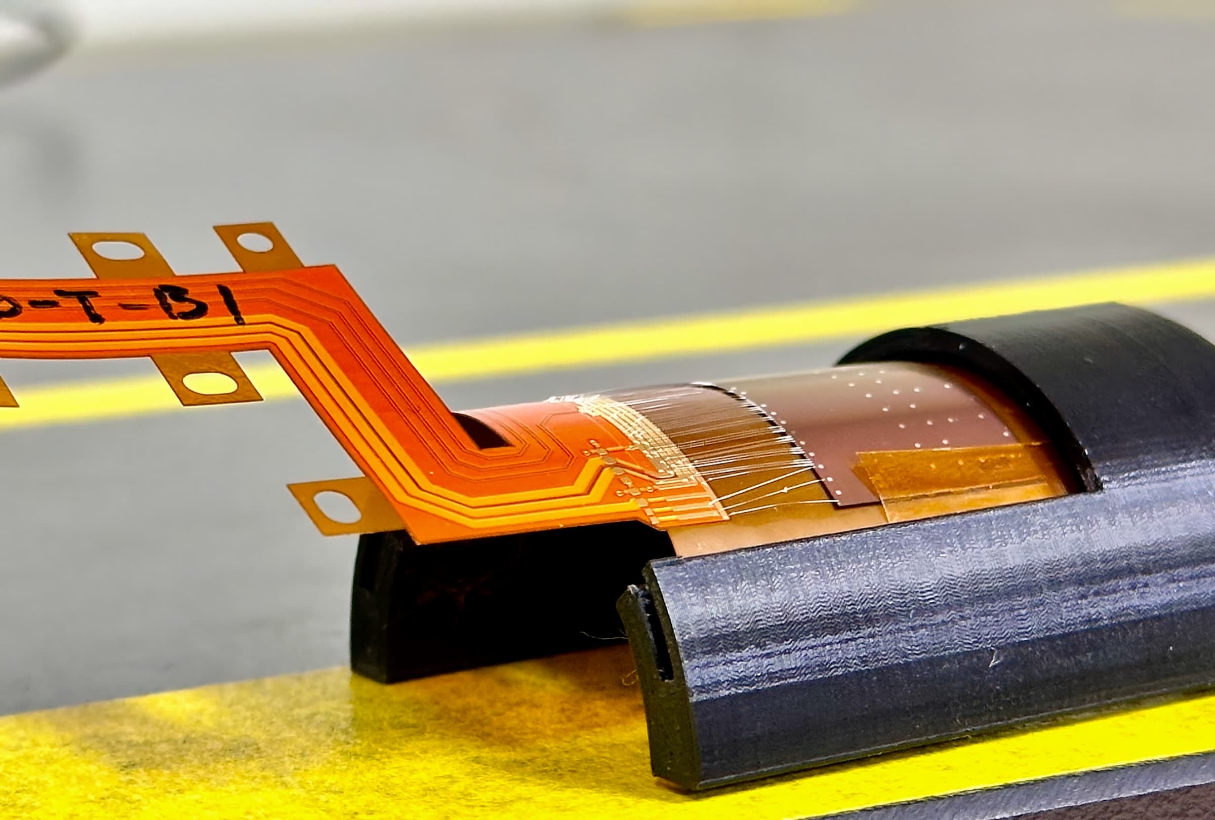
Bent ALPIDE Test Setup

An FPC-bonded ALPIDE mounted on the PNU Guide & Frame and connected through the iBoard, Adapter Board, and DAQ. I used the same chip for standard-scan procedures in flat, bent, and reverse-bent configurations.
Work I Performed
Mounting trials
Used a dummy chip and Kapton tape with different mounting positions and contact areas before handling the FPC test samples.
Fixture design and printing
Designed a Frame with a nominal radius of 18 mm and a Guide for FPC insertion in 3D CAD, then produced test parts with a 3D printer.
Profile measurement
Measured the 3D surface profile of a mounted dummy chip with a Keyence VR-6200 and compared it with the intended geometry.
Readout and scans
Connected the ALPIDE, FPC, iBoard, Adapter Board, and DAQ, then ran the same standard-scan workflow in flat, bent, and reverse-bent configurations.
Measurement Procedure
Conditions and sequence, without results
The test used a 50 μm-thick ALPIDE Bronze sample. Because the DACMONV/I pads were not connected in this assembly, the ALPIDE was used for the DAC Scan. The standard scan types recorded in the presentations were:
- Power Scan
- Analog Scan
- FIFO Scan
- DAC Scan
- Digital Scan
- Scan
- Threshold Scan
After basic checks in the flat configuration, the sample was mounted in the PNU Guide & Frame for the bent configuration. The same types of scans were later run in a reverse-bent configuration. Measurements were taken in a dark room while keeping the settings and sequence as consistent as practical after each configuration change.
The three configurations are named so as to avoid confusion with another group's usage: flat is the unbent chip; bent (forward) has the chip curving outward, the direction another group had been using first; and reverse-bent matches the direction in which ITS3 actually wraps its sensors around the beam pipe. The same fixture was reused to bend several chips in turn, so the procedure could be repeated without handling each sensor directly.
Boundary of my role
This record does not imply that I designed the complete ITS3 detector or performed the ALICE Collaboration's beam tests. My scope was the local test fixture, readout setup, scan execution, and progress presentations at Pusan National University.
Work Timeline
- Mar - Apr 2023: dummy-chip mounting trials and initial Guide-and-Frame CAD work
- May - Jul 2023: PNU Guide & Frame fabrication, VR-6200 profile measurement, and ITS3 WP4 progress presentations
- Aug - Oct 2023: DAQ connection, basic scans, and configuration checks after receiving FPC-bonded samples
- Nov 2023 - Jan 2024: standard scans in flat, bent, and reverse-bent configurations and preparation of presentation materials
Presentation Record
- May 2023, ITS3 WP4 biweekly — “Bending Method Study”
- Jul 2023, ITS3 WP4 biweekly — “Updates on bending methods in Pusan”
- Oct 2023, ITS3 WP4 biweekly — “Bent ALPIDE Updates in Korea”
- Jan 2024, ITS3 WP4 meeting — “Chip bending and interconnection: updates from Korea”
- Jan 2024, KoALICE Workshop — “Study of characteristic changes of Bent ALPIDE”
Tools Used
- 3D CAD and 3D printing
- Keyence VR-6200 3D optical measurement system
- ALPIDE FPC, iBoard, Adapter Board, and DAQ
- ALPIDE standard scans and configuration checks in Linux
Background References
Technical Design Report for the ALICE Inner Tracking System 3 — A bent wafer-scale monolithic pixel detector
ALICE Collaboration
CERN-LHCC-2024-003; ALICE-TDR-021 (2024)
ALPIDE, the Monolithic Active Pixel Sensor for the ALICE ITS upgrade
M. Mager (for the ALICE Collaboration)
Nuclear Instruments and Methods in Physics Research A 824 (2016) 434–438
Testbeam performance results of bent ALPIDE Monolithic Active Pixel Sensors in view of the ALICE Inner Tracking System 3
ALICE ITS3 project
arXiv:2112.10414 (2021)
Updated schedule for CERN's accelerators
CERN
CERN News, 4 October 2024
Accelerator Report: The 2026 run will be short but intense
Bettina Mikulec
CERN News, 12 March 2026
https://home.cern/accelerator-report-2026-run-will-be-short-intense/